แสดงทั้งหมด 4 ผลลัพท์

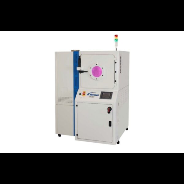
  • Nordson Electronics Solutions – Automated Plasma Treatment System – FlexTRAK® SHS

    Industry-Leading Throughput and Reliability

    Built upon Nordson Electronics Solutions’ patented plasma technology, the FlexTRAK®-SHS is our latest fully automated plasma system incorporating a high-capacity F3-S chamber, to provide ...

    Industry-Leading Throughput and Reliability

    Built upon Nordson Electronics Solutions’ patented plasma technology, the FlexTRAK®-SHS is our latest fully automated plasma system incorporating a high-capacity F3-S chamber, to provide high uniformity and increased productivity. The chamber architecture remains the same as the smaller FlexTRAK platform, providing a seamless transition between chambers as production demands more capacity.

    Key Applications


    • Pre-wire bond plasma treatment on semiconductor package substrates and lead frames
    • Pre-underfill plasma treatment on flip chip packages
    • Pre-mold plasma treatment on semiconductor package substrates and lead frames
    • Plasma treatment of semiconductor package substrates and lead frames for improved adhesion
    • Removal/reduction of oxidation on lead frame
  • Nordson Electronics Solutions – Plasma Polymerization Deposition System – PD Series

    Nordson Electronics Solutions introduces its PD Series Plasma Deposition Systems family, which uses plasma polymerization to deposit thin films uniformly during precision manufacturing and assembly processes to change the surfac...

    Nordson Electronics Solutions introduces its PD Series Plasma Deposition Systems family, which uses plasma polymerization to deposit thin films uniformly during precision manufacturing and assembly processes to change the surface characteristics of a substrate. Plasma deposition can be used for applications in a wide range of industries, including medical, life sciences, industrial, semiconductor, MEMS, plastics, and electronics.

    The PD Series for plasma deposition uses a gas vapor or heated liquid monomer vapor delivery system to deposit coatings that can reduce, and in certain cases eliminate, tackiness, provide a tie layer, make surfaces more slippery or resistant to corrosion, act as a drug enhancement or inhibition agent in life sciences applications, and change desired surfaces from hydrophobic to hydrophilic or vice versa. Polymers can be directly attached to a desired surface while the chains are growing, which reduces the steps necessary for other coating processes such as grafting. This is very useful for pinhole-free coatings of 100 picometers to 1 micrometer thickness with solvent insoluble polymers.

    Key Features

    • Low-temperature processing because plasma energy is the catalyst for film growth.

    • Plasma deposition is uniform and applies coatings evenly over curved or varied-level surfaces.
    • Precise control of film thickness.
    • Eliminates wet chemistry. Because polymers are deposited directly from the monomer, there are no waste streams due to wet chemical synthesis or solvents.
    • Exhibits similar properties to those created via standard chemical polymerization techniques.
    • Can be used in multiple steps during device manufacture: pre-treat the surface, deposit material, and apply functionalized polymer films.
  • Nordson Electronics Solutions – Plasma Systems – Sphere Series

    SPHERE series systems support automated handling and processing of round or square wafer/substrate sizes ranging from 75mm to 300mm. In addition, thin wafer processing with or without carriers is possible, depending upon wafer t...

    SPHERE series systems support automated handling and processing of round or square wafer/substrate sizes ranging from 75mm to 300mm. In addition, thin wafer processing with or without carriers is possible, depending upon wafer thickness.

    The patented plasma chamber design provides exceptional etch uniformity and process repeatability. Primary plasma applications include a variety of etching, ashing, and descum steps. Other plasma processes include contamination removal, surface roughening, increasing wettability, and enhancing bonding and adhesion strength, photoresist/polymer stripping, dielectric etch, wafer bumping, organic contamination removal, and wafer destress.

    • Wafer Cleaning – The SPHERE series plasma systems remove contamination prior to wafer bumping, remove organic contamination, remove fluorine and other halogen contamination, and remove metal and metal oxides. Plasma also improves spun-on film adhesion and cleans metallic bond pads.
    • Wafer Etching – Plasma systems descum wafer of residual photoresist and BCB, pattern dielectric layers for redistribution, strip/etch photoresist, enhance adhesion of wafer applied materials, remove excess wafer applied mold /epoxy, enhance adhesion of gold solder bumps, destress wafer to reduce breakage, improve spun-on film adhesion, and clean aluminum bond pads.
  • Nordson Electronics Solutions – Vacuum Plasma Treatment Systems – AP Series

    AP series plasma treatment machines are suitable for a wide variety of plasma cleaning, surface activation and adhesion improvement applications. These capabilities are used for semiconductor manufacturing, microelectronic packa...

    AP series plasma treatment machines are suitable for a wide variety of plasma cleaning, surface activation and adhesion improvement applications. These capabilities are used for semiconductor manufacturing, microelectronic packaging and assembly, and by manufacturers of medical and life science devices. The AP Series consists of four batch plasma treatment systems offering small, mid-size and large vacuum chamber options that deliver process correlation, controller continuity and reliable, reproducible vacuum gas plasma treatment to customers as they expand from an R&D environment to various levels of production.